Not affiliated with or endorsed by the FCC, NCVEC, ARRL or any VEC. Questions are the NCVEC pools word for word (public domain); explanations are our own. Exam rules and fees can change: check with your VE team.
E6A: Semiconductor materials and devices: semiconductor materials; bipolar junction transistors; operation and types of field-effect transistors
Group E6A of the Amateur Extra pool (2024–2028) has 12 active questions. One of them is on every Amateur Extra exam. Each is shown word for word; open it to see the correct answer and our explanation.
E6A01
In what application is gallium arsenide used as a semiconductor material?
A In high-current rectifier circuits
B In high-power audio circuits
C In microwave circuits
D In very low-frequency RF circuits
Show the answer and explanation
Correct answer: C. In microwave circuits
Why C is right. C. Gallium arsenide lets electrons move faster than silicon does, so its devices work well at microwave frequencies.
Electron mobility is how easily electrons move through a material when a voltage pushes them. GaAs has several times the electron mobility of silicon. Faster electrons mean transistors that amplify at higher frequencies with less noise, which is why GaAs shows up in microwave preamps and amplifiers.
Why not D? Very low frequencies do not need that speed; silicon handles them easily.
E6A02
Which of the following semiconductor materials contains excess free electrons?
A N-type
B P-type
C Bipolar
D Insulated gate
Show the answer and explanation
Correct answer: A. N-type
Why A is right. A. N-type material has extra free electrons, added by donor impurities that carry one more outer electron than silicon.
Pure silicon has four outer electrons per atom, all bound in the crystal. Adding a little phosphorus or arsenic, which have five, leaves one electron free to move. Those free negative charges give N-type its name. P-type instead has missing electrons, called holes.
Why not B? P-type material has extra holes, not extra electrons.
E6A03
Why does a PN-junction diode not conduct current when reverse biased?
A Only P-type semiconductor material can conduct current
B Only N-type semiconductor material can conduct current
C Holes in P-type material and electrons in the N-type material are separated by the applied voltage, widening the depletion region
D Excess holes in P-type material combine with the electrons in N-type material, converting the entire diode into an insulator
Show the answer and explanation
Correct answer: C. Holes in P-type material and electrons in the N-type material are separated by the applied voltage, widening the depletion region
Why C is right. C. Reverse bias pulls holes and electrons away from the junction, widening the depletion region so almost no carriers are left to carry current.
The depletion region is a zone at the junction with no free charge carriers, so it acts like an insulator. Reverse bias draws holes in the P side and electrons in the N side away from the junction. The insulating zone grows wider, and only a tiny leakage current flows.
Why not D? The carriers are pulled apart, not combined, and the whole diode does not become an insulator.
E6A04
What is the name given to an impurity atom that adds holes to a semiconductor crystal structure?
A Insulator impurity
B N-type impurity
C Acceptor impurity
D Donor impurity
Show the answer and explanation
Correct answer: C. Acceptor impurity
Why C is right. C. An acceptor impurity accepts an electron from the crystal, leaving a hole behind.
Atoms such as boron have three outer electrons, one fewer than silicon. In the crystal, each one leaves a gap where an electron could fit. That gap, a hole, can move and carry current like a positive charge. Acceptors make P-type material.
Why not D? Donor impurities give extra electrons, making N-type material.
E6A05
How does DC input impedance at the gate of a field-effect transistor (FET) compare with that of a bipolar transistor?
A They are both low impedance
B An FET has lower input impedance
C An FET has higher input impedance
D They are both high impedance
Show the answer and explanation
Correct answer: C. An FET has higher input impedance
Why C is right. C. An FET's gate draws almost no DC current, so its input impedance is far higher than a bipolar transistor's base.
A bipolar transistor is controlled by base current, so its input must draw current, which means lower input impedance. An FET is controlled by gate voltage. Its gate is a reverse-biased junction (JFET) or is insulated by a thin oxide layer (MOSFET), so very little current flows in.
Why not B? It is the other way around; the bipolar base draws current, so its impedance is lower.
E6A06
What is the beta of a bipolar junction transistor?
A The frequency at which the current gain is reduced to 0.707
B The change in collector current with respect to the change in base current
C The breakdown voltage of the base-to-collector junction
D The switching speed
Show the answer and explanation
Correct answer: B. The change in collector current with respect to the change in base current
Why B is right. B. Beta is current gain: how much the collector current changes for a given change in base current.
In a bipolar transistor, a small base current controls a much larger collector current. If raising the base current by 0.1 mA raises the collector current by 10 mA, beta is 10 / 0.1 = 100. It has no units because it is a ratio of two currents.
Why not A? The frequency where gain drops is a cutoff frequency, not beta.
E6A07
Which of the following indicates that a silicon NPN junction transistor is biased on?
A Base-to-emitter resistance of approximately 6 ohms to 7 ohms
B Base-to-emitter resistance of approximately 0.6 ohms to 0.7 ohms
C Base-to-emitter voltage of approximately 6 volts to 7 volts
D Base-to-emitter voltage of approximately 0.6 volts to 0.7 volts
Show the answer and explanation
Correct answer: D. Base-to-emitter voltage of approximately 0.6 volts to 0.7 volts
Why D is right. D. A silicon base-emitter junction starts conducting at about 0.6 to 0.7 volts, so that reading shows the transistor is on.
The base-emitter junction is a silicon PN junction, like a diode. Below about 0.6 V it conducts very little. Once forward biased to around 0.6 to 0.7 V, base current flows and the transistor turns on. More base current barely changes this voltage.
Why not C? 6 to 7 volts is about ten times the normal forward drop of a silicon junction.
E6A08
What is the term for the frequency at which the grounded-base current gain of a bipolar junction transistor has decreased to 0.7 of the gain obtainable at 1 kHz?
A Corner frequency
B Alpha rejection frequency
C Beta cutoff frequency
D Alpha cutoff frequency
Show the answer and explanation
Correct answer: D. Alpha cutoff frequency
Why D is right. D. The alpha cutoff frequency is where the grounded-base current gain, alpha, falls to about 0.7 of its low-frequency value.
Alpha is the ratio of collector current to emitter current in a grounded-base circuit, a little less than 1. As frequency rises, charge carriers cannot keep up and alpha falls. The point where it reaches 0.707 of its value at 1 kHz, 3 dB down, is the alpha cutoff.
Why not C? Beta cutoff refers to grounded-emitter gain, not grounded-base gain.
E6A09
What is a depletion-mode field-effect transistor (FET)?
A An FET that exhibits a current flow between source and drain when no gate voltage is applied
B An FET that has no current flow between source and drain when no gate voltage is applied
C An FET that exhibits very high electron mobility due to a lack of holes in the N-type material
D An FET for which holes are the majority carriers
Show the answer and explanation
Correct answer: A. An FET that exhibits a current flow between source and drain when no gate voltage is applied
Why A is right. A. A depletion-mode FET conducts from source to drain with zero gate voltage; gate voltage is used to reduce, or deplete, that current.
In a depletion-mode device the channel already exists. Gate voltage of the right polarity narrows it until current stops. An enhancement-mode FET is the opposite: there is no channel at zero gate voltage, and gate voltage must create one. JFETs are always depletion-mode devices.
Why not B? No current at zero gate voltage describes an enhancement-mode FET.
E6A10
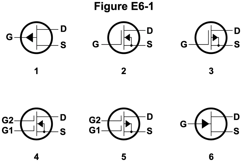
In Figure E6-1, which is the schematic symbol for an N-channel dual-gate MOSFET?
Figure E6-1
A 2
B 4
C 5
D 6
Show the answer and explanation
Correct answer: B. 4
Why B is right. B. Symbol 4 has two gate leads, G1 and G2, and its arrow points inward toward the channel, which marks N-channel.
A MOSFET is an FET whose gate is insulated from the channel. In Figure E6-1, symbols 4 and 5 each have two separate gate lines on the left, labeled G1 and G2, set apart from the vertical channel line by a gap that shows the insulation. The small arrow on the inner line shows channel type. In symbol 4 it points toward the channel: N-channel.
Why not C? Symbol 5 has the same two gates, but its arrow points away from the channel, marking P-channel.
E6A11
In Figure E6-1, which is the schematic symbol for a P-channel junction FET?
Figure E6-1
A 1
B 2
C 3
D 6
Show the answer and explanation
Correct answer: A. 1
Why A is right. A. Symbol 1 is a junction FET whose gate arrow points away from the channel, which marks P-channel.
In Figure E6-1, symbols 1 and 6 are junction FETs: the gate lead, G, touches the vertical channel line directly, with no gap for an insulated gate, and carries an arrowhead. In symbol 1 the arrow points outward, toward the G label, meaning P-channel. In symbol 6 it points inward toward the channel, meaning N-channel.
Why not D? Symbol 6 is also a junction FET, but its arrow points into the channel, so it is N-channel.
E6A12
What is the purpose of connecting Zener diodes between a MOSFET gate and its source or drain?
A To provide a voltage reference for the correct amount of reverse-bias gate voltage
B To protect the substrate from excessive voltages
C To keep the gate voltage within specifications and prevent the device from overheating
D To protect the gate from static damage
Show the answer and explanation
Correct answer: D. To protect the gate from static damage
Why D is right. D. The Zener diodes conduct before static voltage can break through the MOSFET's very thin gate insulation, protecting the gate.
A MOSFET's gate is insulated by a glass-like oxide layer far thinner than a hair. A static spark of a few hundred volts can punch through it and ruin the device. Zener diodes across the gate clamp any voltage above their rating, so the surge flows through them instead.
Why not A? Gate bias comes from the circuit design; the Zeners only clamp surges.