Not affiliated with or endorsed by the FCC, NCVEC, ARRL or any VEC. Questions are the NCVEC pools word for word (public domain); explanations are our own. Exam rules and fees can change: check with your VE team.
E6B: Diodes
Group E6B of the Amateur Extra pool (2024–2028) has 11 active questions. One of them is on every Amateur Extra exam. Each is shown word for word; open it to see the correct answer and our explanation.
E6B01
What is the most useful characteristic of a Zener diode?
A A constant current drop under conditions of varying voltage
B A constant voltage drop under conditions of varying current
C A negative resistance region
D An internal capacitance that varies with the applied voltage
Show the answer and explanation
Correct answer: B. A constant voltage drop under conditions of varying current
Why B is right. B. A Zener diode holds a nearly constant voltage across itself even as the current through it changes.
A Zener is built to break down at a set reverse voltage, such as 5.1 V. Once in breakdown, its voltage barely changes over a wide range of current. That makes it a simple voltage reference or regulator: a resistor sets the current, and the Zener sets the voltage.
Why not D? Voltage-variable capacitance describes a varactor diode.
E6B02
Which characteristic of a Schottky diode makes it a better choice than a silicon junction diode for use as a power supply rectifier?
A Much higher reverse voltage breakdown
B More constant reverse avalanche voltage
C Longer carrier retention time
D Lower forward voltage drop
Show the answer and explanation
Correct answer: D. Lower forward voltage drop
Why D is right. D. A Schottky diode drops only about 0.2 to 0.4 volts when conducting, versus about 0.7 volts for silicon, so less power is wasted as heat.
In a rectifier, the diode's voltage drop times the load current is lost as heat. At 10 A, cutting the drop from 0.7 V to 0.3 V saves about 4 W per diode. Schottky diodes also switch very fast, which suits switching power supplies.
Why not A? Schottky diodes usually have lower reverse voltage ratings, not higher.
E6B03
What property of an LED's semiconductor material determines its forward voltage drop?
A Intrinsic resistance
B Band gap
C Junction capacitance
D Junction depth
Show the answer and explanation
Correct answer: B. Band gap
Why B is right. B. The band gap, the energy an electron gives up crossing the junction, sets both the LED's color and its forward voltage.
In an LED, each electron that drops across the band gap gives off one particle of light. A wider band gap means more energy per particle, a bluer color, and a higher voltage needed to push electrons across. Red LEDs drop about 1.8 V; blue ones about 3 V.
Why not A? Resistance adds a little drop at high current, but the band gap sets the basic forward voltage.
E6B04
What type of semiconductor device is designed for use as a voltage-controlled capacitor?
A Varactor diode
B Tunnel diode
C Silicon-controlled rectifier
D Zener diode
Show the answer and explanation
Correct answer: A. Varactor diode
Why A is right. A. A varactor diode is built to act as a capacitor whose value changes with the reverse voltage across it.
A reverse-biased diode has a depletion region that works like the insulating gap in a capacitor. More reverse voltage widens the gap and lowers the capacitance; less voltage narrows it and raises the capacitance. Varactors let a DC voltage tune oscillators and filters with no moving parts.
Why not D? A Zener holds a steady voltage; its capacitance is not the point.
E6B05
What characteristic of a PIN diode makes it useful as an RF switch?
A Extremely high reverse breakdown voltage
B Ability to dissipate large amounts of power
C Reverse bias controls its forward voltage drop
D Low junction capacitance
Show the answer and explanation
Correct answer: D. Low junction capacitance
Why D is right. D. A PIN diode has very low capacitance when it is off, so it blocks RF well when switched off.
A PIN diode has a wide layer of undoped (intrinsic) silicon between its P and N layers. That wide gap means little capacitance, so little RF leaks through when the diode is off. When forward DC current flows, the middle layer fills with carriers and the diode passes RF with low resistance.
Why not C? Forward DC current, not reverse bias, controls the PIN diode's RF resistance.
E6B06
Which of the following is a common use of a Schottky diode?
A In oscillator circuits as the negative resistance element
B As a variable capacitance in an automatic frequency control circuit
C In power supplies as a constant voltage reference
D As a VHF/UHF mixer or detector
Show the answer and explanation
Correct answer: D. As a VHF/UHF mixer or detector
Why D is right. D. Schottky diodes switch very fast and need little voltage to conduct, which makes them good VHF and UHF mixers and detectors.
A Schottky diode is a metal-to-semiconductor junction. It stores almost no charge, so it can turn on and off extremely quickly. Its low turn-on voltage also helps it detect weak signals. Those traits suit mixers and detectors at high frequencies.
Why not A? The negative resistance element in oscillators is a tunnel diode.
E6B07
What causes a junction diode to fail from excessive current?
A Excessive inverse voltage
B Excessive junction temperature
C Insufficient forward voltage
D Charge carrier depletion
Show the answer and explanation
Correct answer: B. Excessive junction temperature
Why B is right. B. Too much current heats the junction until the semiconductor is damaged, so excess junction temperature is what destroys the diode.
Current through the diode times its voltage drop is power turned into heat. If that heat cannot escape fast enough, the junction temperature climbs. Past the limit, the crystal can melt or crack, leaving the diode shorted or open.
Why not A? Too much reverse voltage is a separate failure, not one caused by excessive current.
E6B08
Which of the following is a Schottky barrier diode?
A Metal-semiconductor junction
B Electrolytic rectifier
C PIN junction
D Thermionic emission diode
Show the answer and explanation
Correct answer: A. Metal-semiconductor junction
Why A is right. A. A Schottky barrier diode is formed where a metal meets a semiconductor, instead of a junction between P-type and N-type material.
The metal-semiconductor contact forms a barrier that lets current pass one way. Since only one type of carrier is involved, there is almost no stored charge to clear when the diode turns off. That gives fast switching and a low forward voltage drop.
Why not C? A PIN junction has P, intrinsic and N layers of semiconductor, with no metal junction.
E6B09
What is a common use for point-contact diodes?
A As a constant current source
B As a constant voltage source
C As an RF detector
D As a high-voltage rectifier
Show the answer and explanation
Correct answer: C. As an RF detector
Why C is right. C. A point-contact diode has a tiny junction with very little capacitance, so it works well as an RF detector.
A point-contact diode is made by pressing a fine wire against a piece of semiconductor. The contact area is tiny, so its capacitance is very small and it responds to high frequencies. It cannot handle much current, which rules out power uses. Early crystal radio sets used this kind of detector.
Why not D? The tiny contact cannot handle high voltage or high current.
E6B10
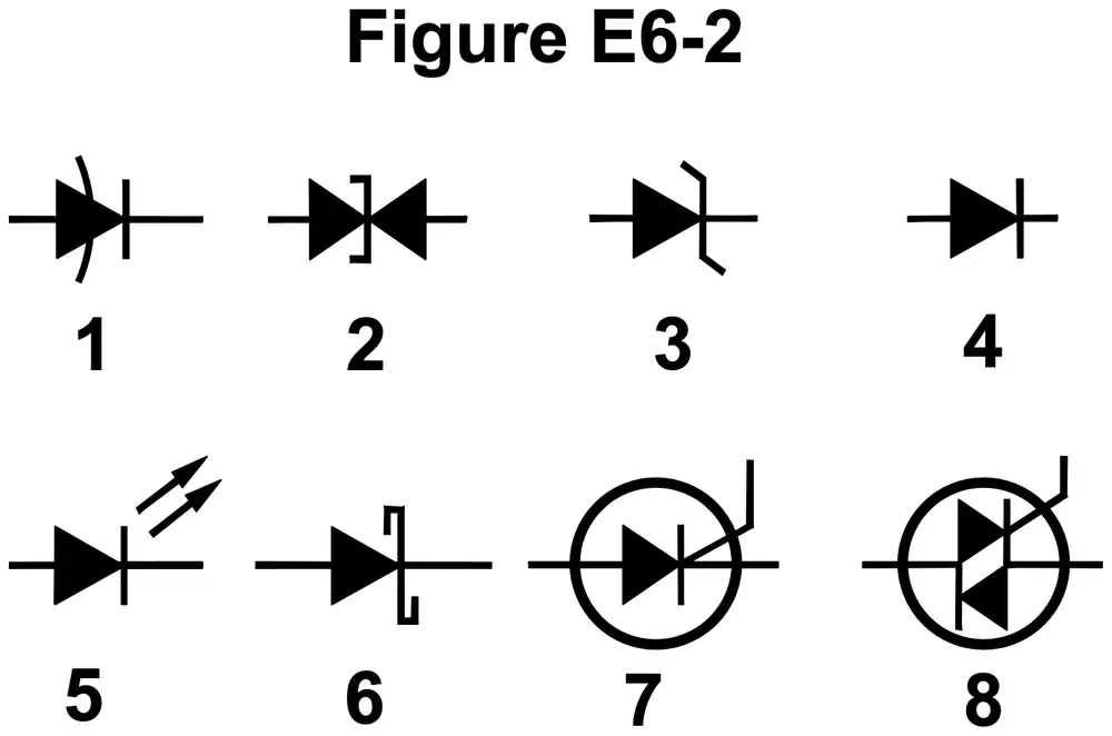
In Figure E6-2, which is the schematic symbol for a Schottky diode?
Figure E6-2
A 1
B 6
C 2
D 3
Show the answer and explanation
Correct answer: B. 6
Why B is right. B. Symbol 6 is a diode whose bar has small square hooks at each end turning in opposite directions, the mark of a Schottky diode.
In Figure E6-2 each diode is a solid triangle pointing at a vertical bar, and the shape of the bar tells the type. In symbol 6 the bar ends in a short hook at the top and another at the bottom, bent opposite ways, like a squared-off S. Symbol 1 instead has a curved arc, and symbol 2 has two triangles meeting at a bracket.
Why not D? Symbol 3's bar has ends slanting off in opposite directions like a Z, the Zener diode symbol.
E6B11
What is used to control the attenuation of RF signals by a PIN diode?
A Forward DC bias current
B A variable RF reference voltage
C Reverse voltage larger than the RF signal
D Capacitance of an RF coupling capacitor
Show the answer and explanation
Correct answer: A. Forward DC bias current
Why A is right. A. The amount of forward DC bias current sets the PIN diode's RF resistance, and so how much the signal is weakened.
Forward current fills the PIN diode's middle layer with charge carriers. More current means more carriers and lower RF resistance. The layer is wide, so the carriers do not clear out within one RF cycle, and the diode acts like a resistor controlled by DC rather than a rectifier.
Why not C? Reverse voltage turns the diode fully off; it does not give adjustable attenuation.