Not affiliated with or endorsed by the FCC, NCVEC, ARRL or any VEC. Questions are the NCVEC pools word for word (public domain); explanations are our own. Exam rules and fees can change: check with your VE team.
E6C: Digital ICs: families of digital ICs; gates; programmable logic devices
Group E6C of the Amateur Extra pool (2024–2028) has 11 active questions. One of them is on every Amateur Extra exam. Each is shown word for word; open it to see the correct answer and our explanation.
E6C01
What is the function of hysteresis in a comparator?
A To prevent input noise from causing unstable output signals
B To allow the comparator to be used with AC input signals
C To cause the output to continually change states
D To increase the sensitivity
Show the answer and explanation
Correct answer: A. To prevent input noise from causing unstable output signals
Why A is right. A. Hysteresis sets two thresholds, one for a rising input and one for a falling input, so small noise near the switching point cannot flip the output back and forth.
Without hysteresis, an input that hovers near the threshold makes the output chatter as noise pushes it across. With hysteresis, once the output switches, the input must move back past a different level to switch it again. That gap ignores small wiggles.
Why not C? Constant switching is the problem hysteresis prevents.
E6C02
What happens when the level of a comparator’s input signal crosses the threshold voltage?
A The IC input can be damaged
B The comparator changes its output state
C The reference level appears at the output
D The feedback loop becomes unstable
Show the answer and explanation
Correct answer: B. The comparator changes its output state
Why B is right. B. A comparator's output switches state when the input crosses the threshold voltage.
A comparator compares two voltages: the input and a reference. If the input is above the reference, the output goes to one state; below it, the output goes to the other. It gives a yes-or-no answer to whether the input is higher.
Why not C? The output is a high or low state, not a copy of the reference.
E6C03
What is tri-state logic?
A Logic devices with 0, 1, and high-impedance output states
B Logic devices that utilize ternary math
C Logic with three output impedances which can be selected to better match the load impedance
D A counter with eight states
Show the answer and explanation
Correct answer: A. Logic devices with 0, 1, and high-impedance output states
Why A is right. A. Tri-state outputs can be 0, 1 or high impedance, which in effect disconnects the output from the line.
Several chips can share one set of wires, called a bus, only if all but one stay silent. In the high-impedance state an output neither pulls the line high nor low; it looks like an open switch. A control pin, often called enable, picks which device drives the bus.
Why not B? Ternary math uses three-valued digits; tri-state logic is still binary with an off state.
E6C04
Which of the following is an advantage of BiCMOS logic?
A Its simplicity results in much less expensive devices than standard CMOS
B It is immune to electrostatic damage
C It has the high input impedance of CMOS and the low output impedance of bipolar transistors
D All these choices are correct
Show the answer and explanation
Correct answer: C. It has the high input impedance of CMOS and the low output impedance of bipolar transistors
Why C is right. C. BiCMOS combines CMOS inputs, which draw almost no current, with bipolar outputs that can drive heavy loads.
CMOS gates have very high input impedance, so they barely load the circuit feeding them. Bipolar transistors can supply large currents quickly, giving low output impedance. BiCMOS builds both kinds on one chip to get the strengths of each.
Why not A? Building two transistor types on one chip makes BiCMOS more complex and costly, not less.
E6C05
Which of the following digital logic families has the lowest power consumption?
A Schottky TTL
B ECL
C NMOS
D CMOS
Show the answer and explanation
Correct answer: D. CMOS
Why D is right. D. CMOS uses paired transistors where one is always off, so almost no current flows except while switching.
Each CMOS gate stacks an N-channel and a P-channel transistor between the supply and ground. In either steady state one of them is off, so there is no steady path for current. Power is drawn mainly while the output changes, which is why CMOS suits battery-powered equipment.
Why not B? ECL keeps its transistors partly on all the time for speed, so it draws a lot of power.
E6C06
Why do CMOS digital integrated circuits have high immunity to noise on the input signal or power supply?
A Large bypass capacitance is inherent
B The input switching threshold is about twice the power supply voltage
C The input switching threshold is about half the power supply voltage
D Bandwidth is very limited
Show the answer and explanation
Correct answer: C. The input switching threshold is about half the power supply voltage
Why C is right. C. A CMOS input switches near half the supply voltage, so noise must swing nearly halfway across the supply to cause a false change.
With a 5 V supply, a CMOS input switches at about 2.5 V. A clean low input sits near 0 V and a clean high near 5 V. Noise of a volt or so cannot push either one across the threshold. This safety gap is called noise margin.
Why not B? A threshold of twice the supply voltage could never be reached, so the input would never switch.
E6C07
What best describes a pull-up or pull-down resistor?
A A resistor in a keying circuit used to reduce key clicks
B A resistor connected to the positive or negative supply used to establish a voltage when an input or output is an open circuit
C A resistor that ensures that an oscillator frequency does not drift
D A resistor connected to an op-amp output that prevents signals from exceeding the power supply voltage
Show the answer and explanation
Correct answer: B. A resistor connected to the positive or negative supply used to establish a voltage when an input or output is an open circuit
Why B is right. B. A pull-up or pull-down resistor ties a line to the positive or negative supply so it has a definite voltage when nothing else drives it.
A logic input left unconnected floats and may read high or low at random from stray noise. A resistor to the positive supply (pull-up) or to ground (pull-down) gives it a default level. When a switch or another output drives the line, it easily overrides the resistor.
Why not A? Key clicks are reduced by shaping the keying waveform, not with pull-up resistors.
E6C08
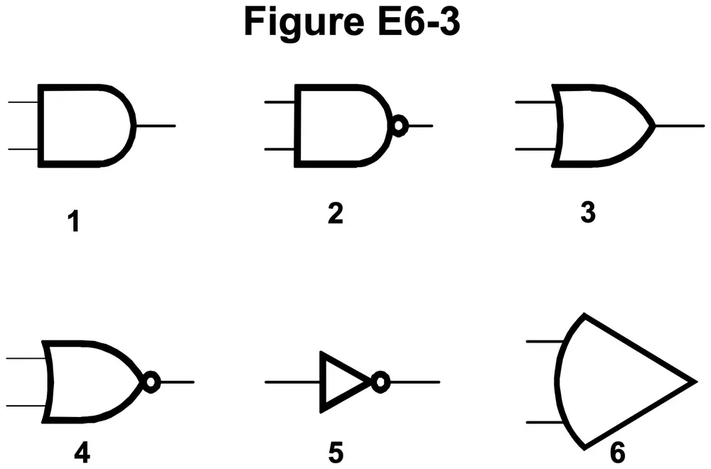
In Figure E6-3, which is the schematic symbol for a NAND gate?
Figure E6-3
A 1
B 2
C 3
D 4
Show the answer and explanation
Correct answer: B. 2
Why B is right. B. Symbol 2 is the AND shape with a small circle at its output, which makes it a NAND gate.
In Figure E6-3, symbol 1 is an AND gate: a D shape, flat on the input side and rounded on the output side, with two inputs. Symbol 2 has the same D shape plus a small circle, or bubble, at the output. The bubble means inversion, so NAND is NOT-AND: its output is low only when both inputs are high.
Why not D? Symbol 4 has the curved, pointed body with a bubble, which is a NOR gate.
E6C09
What is used to design the configuration of a field-programmable gate array (FPGA)?
A Karnaugh maps
B Hardware description language (HDL)
C An auto-router
D Machine and assembly language
Show the answer and explanation
Correct answer: B. Hardware description language (HDL)
Why B is right. B. An FPGA's configuration is written in a hardware description language, such as VHDL or Verilog, that describes the logic circuit.
A field-programmable gate array is a chip full of logic blocks whose connections can be set after it is made. Designers describe the circuit's behavior in HDL. Software then turns that description into a file that sets up the chip's blocks and wiring.
Why not D? Machine and assembly language program a processor, not the wiring of logic blocks.
E6C10
In Figure E6-3, which is the schematic symbol for a NOR gate?
Figure E6-3
A 1
B 2
C 3
D 4
Show the answer and explanation
Correct answer: D. 4
Why D is right. D. Symbol 4 is the curved, pointed OR shape with a small circle at its output, which makes it a NOR gate.
In Figure E6-3, symbol 3 is an OR gate: a curved back where the two inputs enter and a body that sweeps to a point at the output. Symbol 4 has the same shape plus a small circle, or bubble, at the output. The bubble means inversion, so NOR is NOT-OR: its output is high only when both inputs are low.
Why not C? Symbol 3 has no bubble, so it is a plain OR gate.
E6C11
In Figure E6-3, which is the schematic symbol for the NOT operation (inversion)?
Figure E6-3
A 2
B 4
C 5
D 6
Show the answer and explanation
Correct answer: C. 5
Why C is right. C. Symbol 5 is a triangle with one input and a small circle at its tip, the inverter or NOT symbol.
In Figure E6-3, symbol 5 is the only one with a single input. A triangle alone stands for a buffer, which passes a signal unchanged. The bubble at the tip means inversion, so a high input gives a low output and a low input gives a high output.
Why not D? Symbol 6 has two inputs, so it cannot be a single-input NOT gate.