Not affiliated with or endorsed by the FCC, NCVEC, ARRL or any VEC. Questions are the NCVEC pools word for word (public domain); explanations are our own. Exam rules and fees can change: check with your VE team.
E7B: Amplifiers: class of operation; vacuum tube and solid-state circuits; distortion and intermodulation; spurious and parasitic suppression; switching-type amplifiers
Group E7B of the Amateur Extra pool (2024–2028) has 12 active questions. One of them is on every Amateur Extra exam. Each is shown word for word; open it to see the correct answer and our explanation.
E7B01
For what portion of the signal cycle does each active element in a push-pull, Class AB amplifier conduct?
A More than 180 degrees but less than 360 degrees
B Exactly 180 degrees
C The entire cycle
D Less than 180 degrees
Show the answer and explanation
Correct answer: A. More than 180 degrees but less than 360 degrees
Why A is right. A. Class AB is biased slightly on, so each device conducts for its half of the wave plus a little more, between 180 and 360 degrees.
Class A conducts all 360 degrees and class B exactly 180. Class AB sits between. In push-pull, one device handles the positive half and the other the negative half. The small overlap near each zero crossing removes crossover distortion, the kink class B can show where one device hands off to the other.
Why not B? Conduction for exactly 180 degrees is class B.
E7B02
What is a Class D amplifier?
A An amplifier that uses switching technology to achieve high efficiency
B A low power amplifier that uses a differential amplifier for improved linearity
C An amplifier that uses drift-mode FETs for high efficiency
D An amplifier biased to be relatively free from distortion
Show the answer and explanation
Correct answer: A. An amplifier that uses switching technology to achieve high efficiency
Why A is right. A. A class D amplifier drives its transistors fully on or fully off, so very little power is lost as heat.
A switch that is fully on has almost no voltage across it; fully off, it has almost no current through it. Either way, voltage times current, the heat, stays small. The output is a train of pulses whose width or timing carries the signal, and a filter smooths it back into the wanted waveform.
Why not D? Biasing for low distortion describes class A, not a switching design.
E7B03
What circuit is required at the output of an RF switching amplifier?
A A filter to remove harmonic content
B A high-pass filter to compensate for low gain at low frequencies
C A matched load resistor to prevent damage by switching transients
D A temperature compensating load resistor to improve linearity
Show the answer and explanation
Correct answer: A. A filter to remove harmonic content
Why A is right. A. A switching amplifier puts out square-shaped pulses full of harmonics, so a filter must remove them before the antenna.
A square wave contains the fundamental frequency plus odd harmonics at 3, 5 and 7 times that frequency. Those would radiate on other bands and cause interference. A low-pass or band-pass output network passes the operating frequency and rejects the harmonics.
Why not B? The problem is unwanted energy above the operating frequency, not weak gain below it.
E7B04
What is the operating point of a Class A common emitter amplifier?
A Approximately halfway between saturation and cutoff
B Approximately halfway between the emitter voltage and the base voltage
C At a point where the bias resistor equals the load resistor
D At a point where the load line intersects the zero bias current curve
Show the answer and explanation
Correct answer: A. Approximately halfway between saturation and cutoff
Why A is right. A. Biasing midway between saturation (fully on) and cutoff (fully off) lets the output swing equally up and down without clipping.
In class A the transistor conducts for the whole cycle. Placing its resting point, called the Q point, at the center of its range gives the largest undistorted swing both ways. Bias too near either end and one peak flattens. The cost is a steady current even with no signal, so efficiency is low.
Why not B? Bias is set relative to the transistor's on and off limits, not to the gap between emitter and base voltage.
E7B05
What can be done to prevent unwanted oscillations in an RF power amplifier?
A Tune the stage for minimum loading
B Tune both the input and output for maximum power
C Install parasitic suppressors and/or neutralize the stage
D Use a phase inverter in the output filter
Show the answer and explanation
Correct answer: C. Install parasitic suppressors and/or neutralize the stage
Why C is right. C. Parasitic suppressors damp stray VHF resonances and neutralization cancels internal feedback, removing the two main causes of self-oscillation.
An amplifier oscillates when some output leaks back to its input in phase. Capacitance inside the tube or transistor gives such a path; neutralizing adds an equal and opposite feedback to cancel it. Lead inductance and stray capacitance can also resonate at VHF; a parasitic suppressor, often a small coil with a resistor across it, adds loss there.
Why not B? Tuning for maximum power does nothing to remove feedback paths.
E7B06
What is a characteristic of a grounded-grid amplifier?
A High power gain
B Low input impedance
C High electrostatic damage protection
D Low bandwidth
Show the answer and explanation
Correct answer: B. Low input impedance
Why B is right. B. In a grounded-grid stage the drive goes into the cathode, which carries the full tube current, so the input impedance is low.
The control grid is held at RF ground and the signal is applied to the cathode. The driver must supply the whole cathode current swing, so the input looks like a low resistance, often not far from 50 ohms. That makes it easy to drive from a transceiver and very stable.
Why not A? Power gain is only moderate, because much of the drive power passes straight through to the output.
E7B07
Which of the following is the likely result of using a Class C amplifier to amplify a single-sideband phone signal?
A Reduced intermodulation products
B Increased overall intelligibility
C Reduced third-order intermodulation
D Signal distortion and excessive bandwidth
Show the answer and explanation
Correct answer: D. Signal distortion and excessive bandwidth
Why D is right. D. Class C conducts for well under half a cycle and does not track amplitude, so an SSB signal comes out distorted and spread wide.
SSB carries its information in changing amplitude. A class C stage is nonlinear: its output does not rise and fall in proportion to its input. That bending of the waveform creates new frequencies, called intermodulation products, that widen the signal and garble the audio. SSB needs a linear amplifier, class A, AB or B.
Why not A? Nonlinearity creates more intermodulation products, never fewer.
E7B08
Why are switching amplifiers more efficient than linear amplifiers?
A Switching amplifiers operate at higher voltages
B The switching device is at saturation or cutoff most of the time
C Linear amplifiers have high gain resulting in higher harmonic content
D Switching amplifiers use push-pull circuits
Show the answer and explanation
Correct answer: B. The switching device is at saturation or cutoff most of the time
Why B is right. B. A switch is fully on (saturation) or fully off (cutoff) almost all the time, so voltage across it and current through it are rarely large together.
Heat in a transistor equals the voltage across it times the current through it. A linear amplifier keeps the device partly on, with both values sizable, so it wastes power. A switch spends little time in that middle region, so its efficiency can top 90 percent.
Why not D? Linear amplifiers often use push-pull too, so that is not where the saving comes from.
E7B09
What is characteristic of an emitter follower (or common collector) amplifier?
A Low input impedance and phase inversion from input to output
B Differential inputs and single output
C Acts as an OR circuit if one input is grounded
D Input and output signals in-phase
Show the answer and explanation
Correct answer: D. Input and output signals in-phase
Why D is right. D. The output is taken from the emitter, which follows the base voltage up and down, so output and input stay in phase.
In a common-collector stage the emitter sits about 0.6 volt below the base and tracks it. Voltage gain is a little under 1, but current gain is high. Input impedance is high and output impedance is low, which makes it a good buffer between stages.
Why not A? An emitter follower has high input impedance and no inversion; inversion belongs to the common-emitter stage.
E7B10
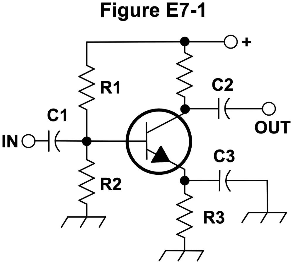
In Figure E7-1, what is the purpose of R1 and R2?
Figure E7-1
A Load resistors
B Voltage divider bias
C Self bias
D Feedback
Show the answer and explanation
Correct answer: B. Voltage divider bias
Why B is right. B. R1 and R2 split the supply voltage and hold the transistor's base at a steady DC level, which sets its bias.
In Figure E7-1, R1, a zigzag resistor, runs from the positive supply line down to the base of the transistor, and R2 runs from that same base point to ground. The input signal reaches this point through C1, the capacitor drawn as a straight line and a curved line. The fraction of supply voltage between the two resistors sets the base bias.
Why not D? Neither resistor connects the output back to the input, so neither one gives feedback.
E7B11
In Figure E7-1, what is the purpose of R3?
Figure E7-1
A Fixed bias
B Emitter bypass
C Output load resistor
D Self bias
Show the answer and explanation
Correct answer: D. Self bias
Why D is right. D. R3, in the emitter lead, develops a voltage from the transistor's own current that sets and steadies the bias.
In Figure E7-1, R3 is the zigzag resistor from the transistor's emitter, the lead with the arrow, to ground. Emitter current makes a voltage across R3. If current rises, for example from heat, that voltage rises, the base-to-emitter voltage shrinks, and current is pulled back down. The bias corrects itself.
Why not B? Emitter bypassing is done by C3, the capacitor from the emitter to ground, not by R3.
E7B12
What type of amplifier circuit is shown in Figure E7-1?
Figure E7-1
A Common base
B Common collector
C Common emitter
D Emitter follower
Show the answer and explanation
Correct answer: C. Common emitter
Why C is right. C. The signal enters at the base and leaves from the collector, while the emitter is tied to ground for signals, so the emitter is the common lead.
A transistor stage is named for the lead shared by input and output. In Figure E7-1, the input passes through capacitor C1 to the base, and the output comes from the collector through capacitor C2 to OUT. The emitter goes to ground through R3, with capacitor C3 across R3 grounding it for signals.
Why not B? Common collector, also called emitter follower, would take its output from the emitter, not the collector.